The Liquid Crystal Display (LCD) is used to display the character that is represented as the American Standard Code for Information Interchange (ASCII) values. The ASCII values are 8-bit (0-7). The ASCII value can be shown in Fig. 1.

Fig. 1. ASCII Code
In this ASCII case, to make character “a” the number shall be 61H and the character “A” shall be 41H, and so on. The 16×2 LCD with 5×8 pixel matrix (per character) means that the LCD contains 2 rows and 16 characters and can be displayed per line. The single character displayed in 5×8 pixel matrix. The configuration of this LCD is shown in Fig. 2.

Fig. 2. LCD Configuration
The details of the LCD configuration could be shown in Table 1.
Table 1. Details of LCD Configuration
| Pin |
Name | Function | Description |
| 1 | Vss | Power supply | Ground |
| 2 | Vdd | Power supply | +5v |
| 3 | Vo | Contrast adjust | 0-5v |
| 4 | RS | Command | Register select |
| 5 | RW | Command | Read /Write |
| 6 | E | Command | Enable |
| 7 | DB0 | Input/Output | Data(LSB) |
| 8 | DB1 | Input/Output | Data |
| 9 | DB2 | Input/Output | Data |
| 10 | DB3 | Input/Output | Data |
| 11 | DB4 | Input/Output | Data |
| 12 | DB5 | Input/Output | Data |
| 13 | DB6 | Input/Output | Data |
| 14 | DB7 | Input/Output | Data(MSB) |
| 15 | A | LED+ BKL | +5v |
| 16 | K | LED- BKL | Ground |
The Functions of LCD could be defined as bellow:
- Power Supply: the first two pins of LCD must be connected to +5V and 0V.
- Vo: the V0 pin is a contrast pin used to set the contrast of LCD using variable resistor (VR) about 10K in range 0-5V.
- Register Select (RS): the RS is a command pin for the LCD. The LCD command and RW operations are set by RS pin. The LCD consists of two registers i.e. the data and command register. When command writes on the LCD, the data register is used. When the data either read or write on the LCD, the command register is used. The selections of register are determined by the logic status of RS. If the logic state of RS is ‘1’, the data register is selected. If the logic state of RS is ‘0’, the command register is selected.
- Enable: When the data send to data pins of LCD, the high to low pulse will be given.
- Data Pins (DB0-DB7): The DB0-DB7 is data input/output (I/O) pins. The LCD is accepted the 8 bit data as a parallel form. The format of data stream is first bit must be LSB bit continue it the other bits are sent. The LCD supports only an ASCII value.
- LED Backlight: The pin no’s 15 and 16 are allocated for LCD backlight. The supply of LED backlight is +5V and 0V. It makes a brightness of the LCD display. The LED backlight pins are denoted as (Anode (A), Cathode (K)) on the LCD.
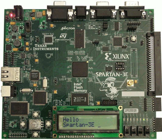
For summary, The LCD consists of 8-Data lines 0f DB0-DB7, RS- Register Select line, RW-Read Write line, and En- Enable line (See Fig. 3).
The initialization to display characters to the LCD, First the LCD requires to send commands to initialize the display, Curser Position, Clear Display, increment curser etc. All this command are send to instruction Register. Instruction Register can be enabled by RS = ‘0’, RW = ‘1’, En= ‘1’. The ASCII codes to command in the FPGA are shown in below,
38 = Function Set: 8-bit, 2 Line, 5×7 Dots
0c = Display on Cursor off
06 = Entry Mode
01= Clear Display
C0 = Place Curser to 2nd line
After sending commands, Data can be transferred to Display in the LCD. For sending, Data enable and Data Register by sending RS= ’1’, RW= ‘1’, En= ’1’.
Data can be transferred in 2 ways 8-bit mode and 4-bit mode and for interfacing in 8-bit mode with the entire Data pin DB0-DB7.

Fig. 3. Interfacing FPGA
For 16×2 LCD VHDL code download, please click here.


